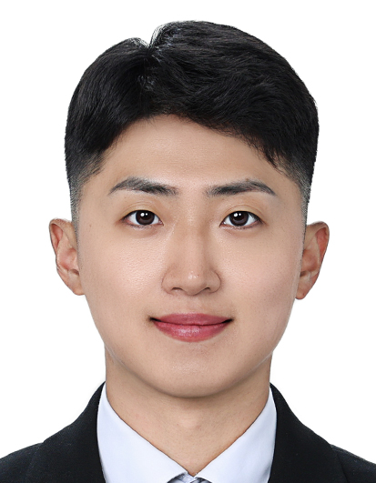
Career Profile
Sunghoon Kim is a Staff Engineer at Samsung Electronics (Foundry).
He received a Master of Science degree in Electrical Engineering from Pohang University of Science and Technology (POSTECH), Korea, in August 2020. Advisor was Prof. Seokhyeong Kang in CAD & SoC Design Lab.
At Samsung Foundry, his work focuses on backend-flow optimization and circuit PPA optimization, with broader work in AI/ML-driven EDA methodologies, LLM-based engineering automation, standard-cell modeling, and AI-based yield ramp-up.
At POSTECH, his research focused on energy-efficient deep learning computing at the intersection between machine learning and low-power VLSI design.
Before joining POSTECH, he received a Bachelor of Science degree with the highest honors in Materials Science Engineering and Electrical & Electronic Engineering at Ulsan National Institute of Science and Technology (UNIST), Korea in February 2018.
– Last update Jul. 2026 –
Experiences
- Lead and contribute to AI/ML-based backend-flow optimization and circuit PPA methodologies for semiconductor implementation.
- Develop reusable design automation workflows across EDA methodology, circuit modeling, and engineering productivity.
- Evaluate LLM-based workflows for EDA assistance, design knowledge reuse, and engineering process automation.
- Collaborate with design, CAD, and methodology teams to turn research prototypes into practical internal flows.
- Developed AI/ML methodologies for backend-flow improvement, circuit PPA optimization, and foundry yield ramp-up.
- Built data analysis, model evaluation, and explainability workflows for semiconductor design and process data.
- Contributed to cross-functional projects across design automation, EDA methodology, and productivity enhancement.
- Thesis: MDARTS: Multi-objective Differentiable Neural Architecture Search
Projects
- Drove AI-assisted design-space exploration for advanced circuit implementation flows.
- Connected commercial EDA optimization engines with internal methodology to improve timing, power, area, routability, and flow productivity trade-offs.
- Collaborated with design and CAD teams to translate experiment learnings into reusable flow guidance without exposing confidential design details.
- Evaluated LLM-based assistants and workflow automation for circuit design, EDA troubleshooting, documentation search, and engineering knowledge reuse.
- Designed prompt and workflow patterns that connect internal knowledge, tool logs, and engineering procedures while respecting confidentiality boundaries.
- Explored agentic workflows to reduce repetitive analysis and improve collaboration between design, CAD, and methodology engineers.
- Designed a heterogeneous graph neural network methodology for standard-cell delay prediction by modeling circuit elements, parasitics, connectivity, and operating conditions as graph-structured inputs.
- Built an explainability workflow to identify transistor, RC, edge, and critical-net factors behind model predictions and align model behavior with circuit-engineering insight.
- Automated training, hyperparameter search, fine-tuning, inference, and reproducibility workflows to complement SPICE-based analysis and reduce repetitive simulation exploration.
- Developed a machine-learning methodology to predict likely design-rule issues earlier in backend implementation flows.
- Built feature engineering, model evaluation, and explainability workflows to help engineers prioritize risky regions and plan iterations.
- Contributed to research dissemination through an engineer-track publication.
- Developed ML pipelines for semiconductor data preprocessing, yield prediction, cause analysis, and experiment prioritization.
- Applied explainable AI and statistical analysis to help engineering teams interpret process and design signals.
- Contributed to an award-winning internal methodology for foundry yield ramp-up.
Papers
- ML-based PPA Push using DRV Prediction
- MDARTS Multi-objective Differentiable Neural Architecture Search
- GRLC Grid-based Run-length Compression for Energy-efficient CNN Accelerator
- Spatial Correlation-aware Compression Algorithm for Saving DRAM Access Energy
- Analysis and Solution of CNN Accuracy Reduction over Channel Loop Tiling
- Analysis and Solution of CNN Accuracy Reduction over Channel Loop Tiling
Patents
NEURAL NETWORK ACCELERATOR AND OPERATING METHOD THEREOF
United States Patent US11960986B2, Granted on Apr. 16, 2024, link2, Transfer of patent to Samsung Electronics with reward
Awards
Samsung Electronics Co., Ltd Annual Awards in S/W Division Silver Prize, 2022.12.29 (삼성전자), AI-based Foundry Yield Ramp-up Methodology Development
Best paper award at ISLPED, 2020 link
Excellent paper award in VLSI CAD division at KCS, 2020
Best paper award at ISE Conference, 2018
Graduated with highest honors from UNIST: GPA (4.17/4.3), 2018 link
Kyungdong Scholarship for Harvard-UNIST Summer Exchange Program 2017 link
Republic of Korea National Science and Engineering Scholarship, 2012 - 2018
Teachings
I am a teaching assistant for the following courses:
Instructor for the SW CERTIFICATION PRO Exam Preparation Course at Samsung Electronics (Jul. 11-12, 2024), 삼성 소프트웨어 인증 PRO 시험 대비반 강사 출강
Mentored interns in the Samsung Talent Internship Program, providing technical guidance and career advice (Jul. 2024 - Aug. 2024), 삼성 수재인턴십 멘토 수행
Served as a Senior Samsung Value Program (SVP) as part of the Leadership Development Course (Feb. 2024 - Mar. 2024), 삼성 신입사원 연수프로그램 (SVP) 선배 수행
EECE490F: Introduction to VLSI Design, Spring 2019 at POSTECH
Manage CSDL Tutorial Page: https://github.com/CSDL-postech/CSDL_Tutorial
My Study Page: https://github.com/kim-sunghoon/Study-materials